Infrared visualization technology has found extensive applications in fields such as security surveillance, medical diagnostics, and industrial inspection. Traditional infrared imaging typically relies on integrating detector arrays, such as indium gallium arsenide (InGaAs), with readout integrated circuits (ROICs), followed by complex image processing workflows to produce images. This process demands stringent flip-chip bonding, constraining pixel size and scalability while significantly increasing costs.
In recent years, upconversion infrared detectors—formed by physically stacking solution-processed infrared photodetectors with visible light-emitting diodes (LEDs)—have garnered attention due to their simple fabrication process and relatively low cost. However, existing infrared upconversion photodetectors suffer from low photon conversion efficiency, poor contrast between illuminated and dark states, and small device areas, severely hindering their imaging performance.
As a prospective solution to this challenge, recently, Professor Ning Zhijun’s team from the School of Physical Science and Technology (SPST) at ShanghaiTech University developed an infrared upconversion imager based on infrared colloidal quantum dots and perovskite visible LEDs. This innovation not only achieves a high-resolution, large-area infrared imaging device with an equivalent pixel count exceeding 7 million but also enables direct infrared visualization of confidential information. The findings were published online in the academic journal Device on February 14.

Figure 1: Schematic of the upconversion detector structure.
Building on their prior research into quantum dot-based infrared upconversion devices, Ning’s team identified that the low efficiency of traditional quantum dot upconversion detectors stemmed primarily from the low luminescence efficiency of the emitting layer. A key factor was the energy level mismatch between the colloidal quantum dot photodetector and the emitting layer, which impaired carrier transport from the infrared detector to the LED, consequently reducing carrier injection into the emitting layer.
To address this, the team replaced the conventional quantum dot emitting layer with an emerging halide perovskite material. The valence band maximum of perovskite LEDs is 0.5 eV lower than that of quantum dot LEDs, significantly reducing the energy barrier between the infrared photodetector and the LED. This enhancement greatly improved hole transport through the intermediate layer. Space-charge-limited current (SCLC) measurements revealed that the hole density in the hole-only transport layer of perovskite LED devices was approximately two orders of magnitude higher than that in quantum dot LEDs. This improved hole transport balances electron and hole injection into the LED layer, markedly boosting the external quantum efficiency of the perovskite LED.
The resulting infrared upconversion device, combining infrared quantum dots and perovskite emitters, achieves an infrared-to-visible photon conversion efficiency of 10.6%. Additionally, the device exhibits a gain exceeding 10 under infrared illumination, yielding high contrast between illuminated and dark states. Coupled with its elevated gain and photon conversion efficiency, the device’s resolution is substantially enhanced. Mask-based testing demonstrated that the upconversion detector can resolve line pairs up to 43.5 lp/mm, corresponding to an 11 μm resolution—the highest reported value for solution-processed infrared upconversion devices to date.
Beyond efficiency and resolution gains, this work also realized large-area imaging. The team utilized a liquid-phase surface ligand exchange process to prepare quantum dot ink for infrared-sensitive films, improving film uniformity compared to traditional solid-phase ligand exchange methods. Using this quantum dot film, they fabricated an ultra-large-area upconversion imaging device with a working area of 9 cm²—far surpassing the areas of previously reported infrared upconversion devices and exceeding the sensor area of full-frame cameras (8.64 cm²). Based on the detector’s spatial resolution and area, the equivalent pixel count of this large-area upconversion device exceeds 7 million, surpassing the maximum pixel count of current CMOS-based infrared imagers.
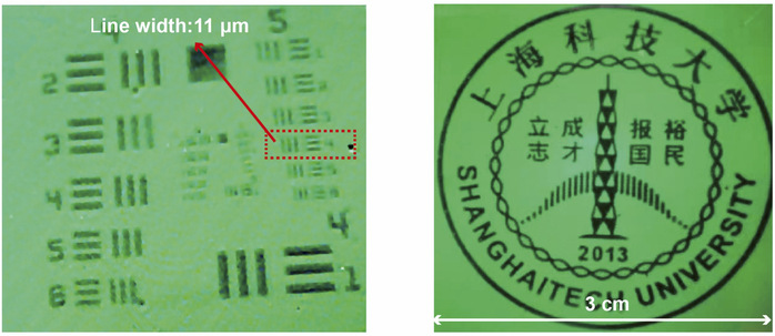
Figure 2: Resolution test image of the infrared upconversion detector (left) and infrared visualization of the ShanghaiTech University emblem using the upconversion detector (right).
The device’s high resolution and large working area make it suitable for direct visualization imaging. The team successfully demonstrated high-definition infrared imaging of the ShanghaiTech University emblem (Figure 2). Furthermore, the device can image confidential information concealed between two opaque substrates (Figure 3), clearly revealing hidden “SHT” text through the upconversion detector.
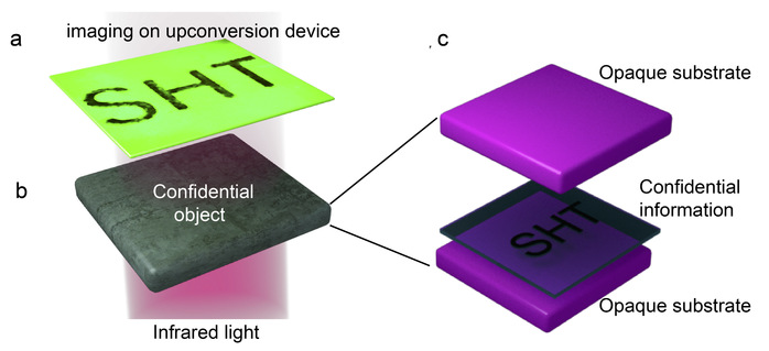
Figure 3: Schematic of the upconversion detector imaging a concealed pattern.
This work establishes a novel infrared upconversion device architecture by integrating infrared quantum dot photodetectors with perovskite emitting materials. The new structure delivers exceptional photon upconversion performance, enabling applications in infrared imaging and information security, with promising development prospects. A patent has been filed for this innovation. Additionally, the study demonstrates that lowering the energy barrier between the infrared photodetector and the LED can significantly enhance the LED’s luminescence quantum efficiency, thereby improving the photon-to-photon conversion efficiency and imaging quality of upconversion detectors. This insight offers a valuable direction for the future development of upconversion technology.
ShanghaiTech University is the primary affiliation for this achievement. PhD graduate Wang Hao, master’s student Liu Yunlong, and Research Associate Professor Zhou Wenjia from Ning’s group are co-first authors, with Prof. Ning Zhijun as the corresponding author.